What I learned in...
EMC & Packaging Lab Research Internship
1. Overview
During my internship at the KCC EMC & Packaging Research Lab, I explored semiconductor packaging processes, EMC (Epoxy Molding Compound) materials, and PCB/Solder Resist workflows. Through lectures and hands-on experiments, I gained practical understanding of how material properties influence the reliability and performance of semiconductor devices.
2. What I Worked On
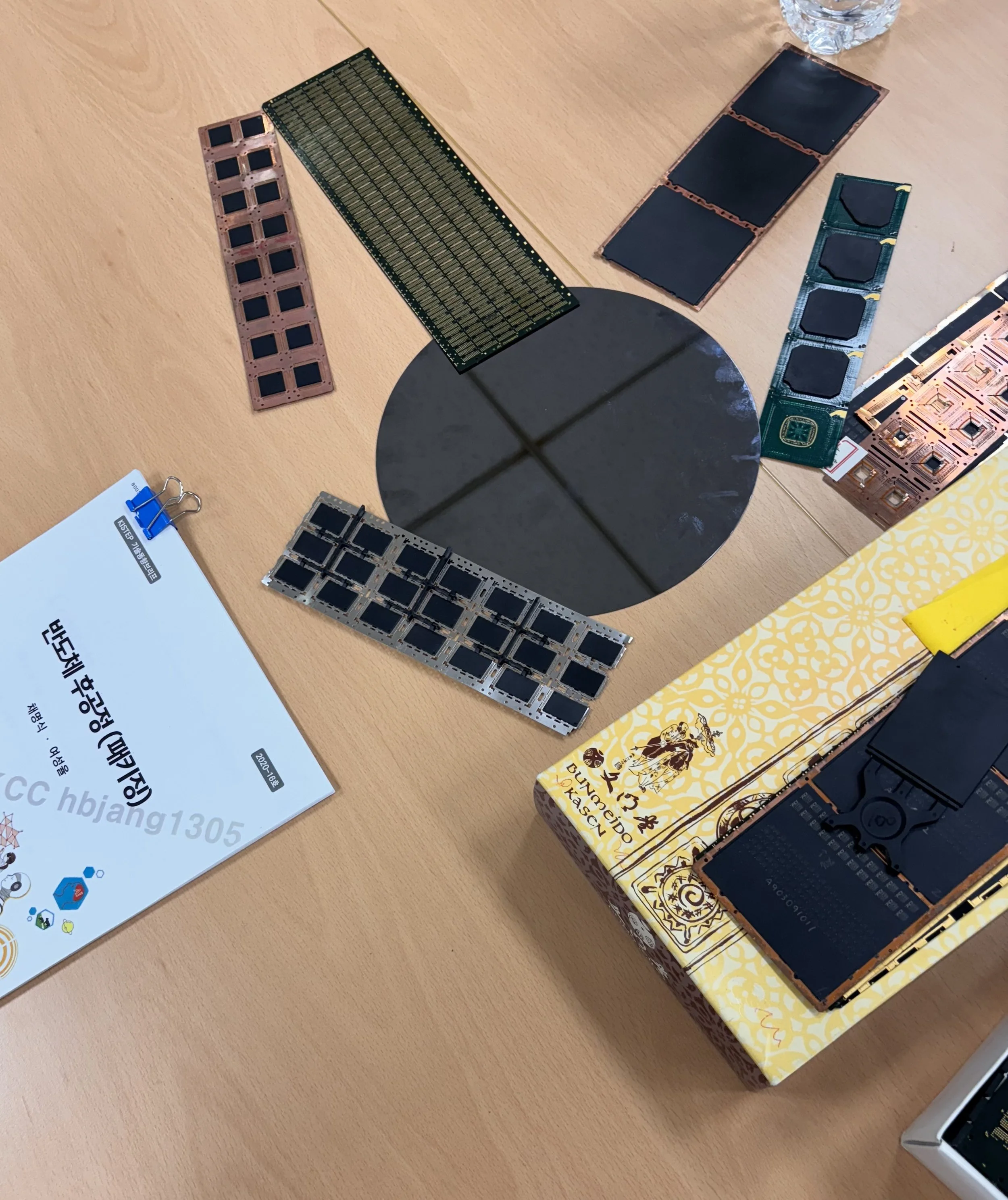
Semiconductor Packaging Fundamentals
- Wafer fabrication, oxidation, photolithography, etching, metallization
- Wire bonding vs. flip-chip bonding
- Packaging structure and reliability considerations
Epoxy Molding Compound (EMC)
- Learned EMC injection and granule molding processes
- Analyzed defect mechanisms: voids, wire sweep, incomplete fill, shrinkage
- Studied key material metrics: Spiral flow, Viscosity & gel time, Hot hardness, Thermal expansion (TMA)
Hands-On Experiments
- Operated molding equipment and measured EMC properties
- Tested flow, curing behavior, thermal expansion
- Observed and compared molding outcomes under different conditions
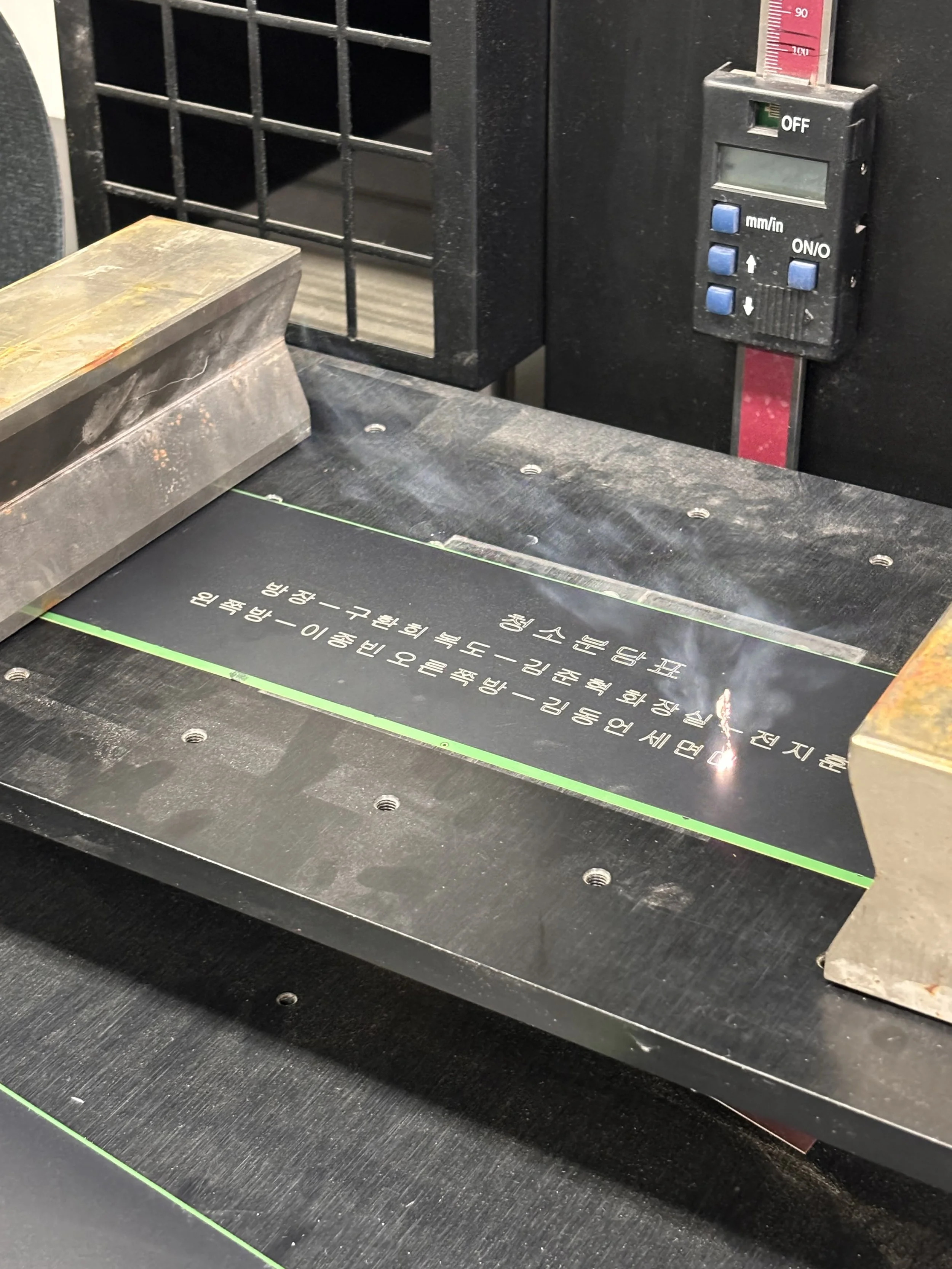
Solder Resist (SR) & PCB Fabrication
- Studied SR coating, UV exposure, development, post-cure
- Mixed SR ink and measured viscosity and curing temperature
- Designed and engraved PCB patterns using laser tools